
Controlled Impedance PCB Manufacturing
0.1 mm off changes how a trace fails at speed. We measure impedance, we don’t assume it.
Tolerance Explained
What Controlled Impedance PCB Manufacturing Actually Controls
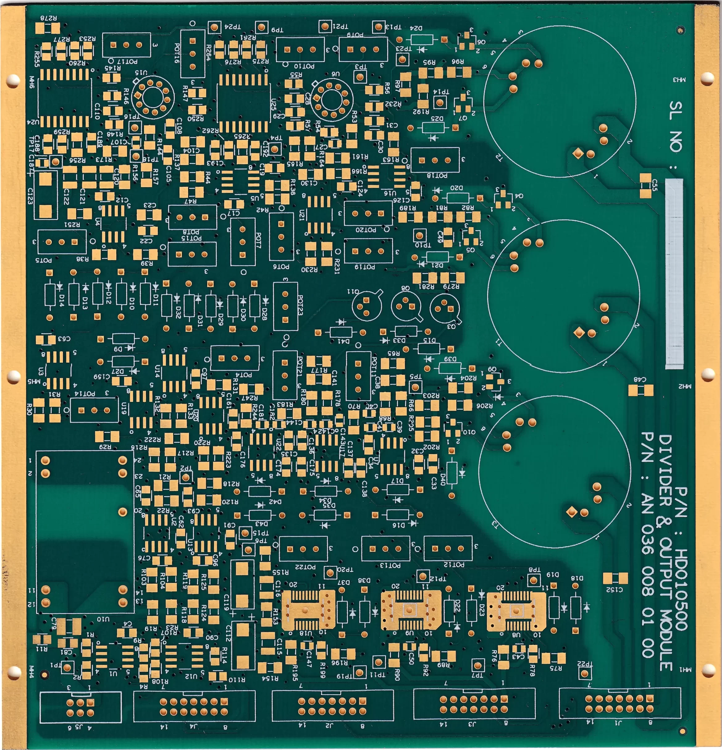
Controlled impedance PCB manufacturing holds trace impedance within a set tolerance by controlling trace width, copper thickness, dielectric height, and laminate dielectric constant together. Get the combination wrong, and a 50-ohm trace reads 46, and the signal reflects instead of passing through clean.
High-speed PCB and high frequency PCB designs cannot absorb that kind of mismatch. Differential impedance PCB pairs also need matched length and spacing, or the signal degrades before reaching the receiver. Signal integrity PCB design is decided at fabrication, not only in the schematic. PC Process builds PCB signal integrity solutions around two failure points that matter most at speed.
Signal Reflection
Differential Pairs
Every Unit Verified
How PC Process Holds Impedance Tolerance
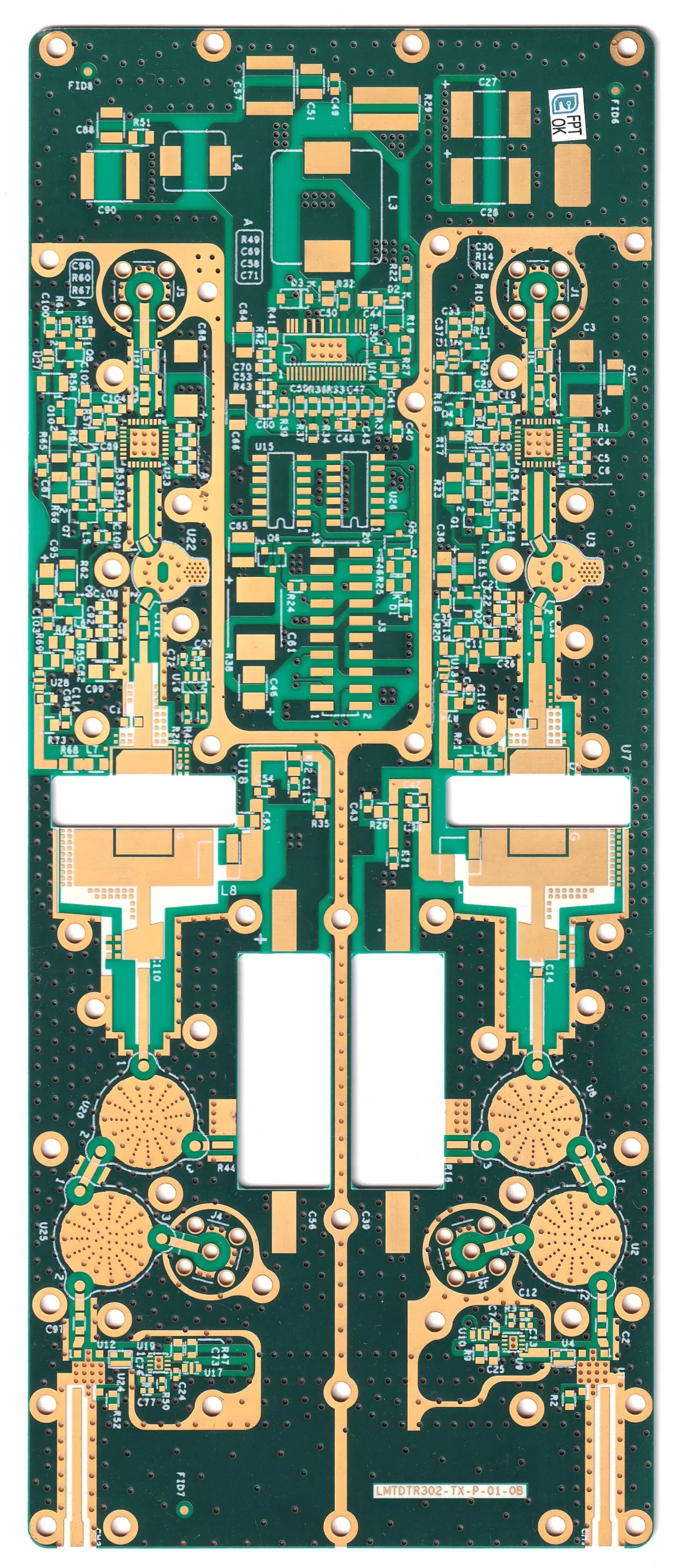
Controlling impedance on paper is easy. Holding it across a production run is the real problem. PC Process runs Laser Direct Imaging on outer layers for sub-25 micron accuracy, keeping trace geometry (and the impedance it sets) consistent panel to panel.
Every board gets impedance measured before shipping, on every unit, not a sampled batch. Multilayer controlled impedance PCB and Rogers builds run the same in-house pipeline, from DFM review through final test, the same precision PCB manufacturing standard applied regardless of layer count.
- LDI sub-25 micron accuracy
- Per-unit impedance testing
- FR4 and Rogers substrates
- Multilayer up to 24 layers
- In-house DFM to final test
- ENIG and HASL finishes
Fabrication Range
Controlled Impedance PCB Capabilities
From single prototypes to volume production, one process, one facility, one quality standard throughout.
Impedance Tolerance Verification
Measured per unit via inline impedance testing, not sampled from a batch.
Multilayer Impedance Stack-Ups
Consistent dielectric and copper control across multilayer controlled impedance PCB builds up to 24 layers.
FR4 and Rogers Substrate Options
Standard digital builds and high frequency PCB builds on Rogers material, both fabricated in-house.
LDI-Driven Trace Precision
Sub-25 micron outer-layer accuracy, on which the geometry-based impedance tolerance depends.
Order Pathway
Getting a Controlled Impedance PCB Quote
Three steps from Gerber upload to a verified board: review, confirm, and fabricate, the same controlled impedance PCB fabrication path every high-speed controlled impedance PCB order runs through before it ships.
Step 1
Send Your Stack-Up
Upload Gerbers with target impedance values and stack-up specs.
Step 2
Engineer Reviews Your Files
An engineer reviews stack-up for DFM and impedance feasibility.
Step 3
Fabrication and Verification
Production runs in-house, with impedance verified before shipping.
Industry Fit
Where Controlled Impedance PCBs Get Used
A backplane and a radar link both need PCB signal integrity solutions, but they fail in different ways when the design falls short. Demand for controlled impedance PCB fabrication in Bangalore is concentrated in a few sectors where the electrical margin for error is extremely thin, and India-wide demand tracks the same pattern.
Telecom and IT Infrastructure
High-speed backplanes run on tight timing budgets. A mismatch shows up as packet loss or link instability, not a visible fault.
Defence and Aerospace
RF and radar links depend on matched impedance for signal fidelity over distance. LCSO-certified under JSS 52302 for defence.
Medical Electronics
Diagnostic imaging moves high-speed data through compact multilayer boards. Here, a signal failure is a diagnostic one.
Industrial Automation
High-speed control buses coordinate equipment in real time. A reflected signal can desynchronise the system it runs.
Trusted Since 1983
PCB Manufacturer Trusted by India's Toughest Industries
Four decades of high-speed PCB manufacture and impedance-controlled fabrication doesn’t mean much without the names behind it. PC Process has built boards for ISRO through VSSC, HAL, and BEL, alongside private-sector names including Bosch, Siemens, and Texas Instruments across defence, aerospace, telecom, and medical electronics.
These aren’t logos on a page. They’re organisations that sent PC Process their highest-consequence builds and came back for the next one.






















What is a controlled impedance PCB?
Why does controlled impedance matter for high-speed PCB design?
Does PC Process manufacture controlled impedance PCBs on Rogers material?
How is impedance verified on a finished board?
Can PC Process fabricate controlled impedance boards for defence programs?
What's the difference between single-ended and differential impedance control?
Does PC Process offer controlled impedance PCB manufacturing in Bangalore for multilayer builds?
Common Questions

