
Multilayer PCB Manufacturer in Bangalore
Every layer you add to a board is another chance for something to drift out of place.
Layer Logic
Multilayer PCB Stack-Up Design That Holds Under Load
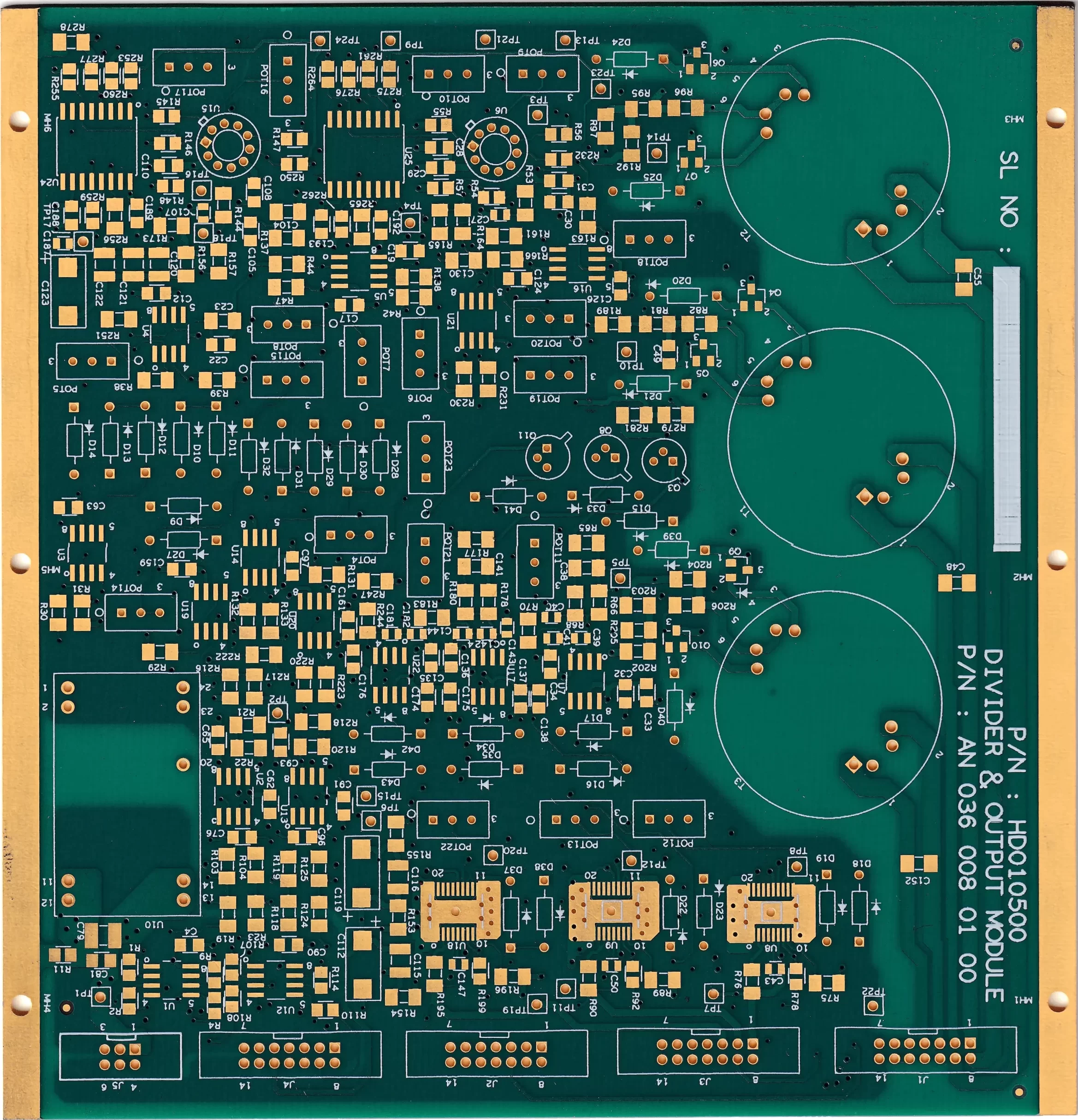
We fabricate up to 24 layers using laminate stack-ups matched to your board’s electrical and mechanical requirements: FR4 for standard multilayer builds, Rogers substrates where high-frequency performance calls for it. Stack-up planning happens before the first panel is cut, not adjusted mid-run, because a stack-up decided late is a stack-up that compromises later.
As a high layer count PCB manufacturer, registration accuracy is the variable that decides whether a 24-layer board actually performs as designed. We use Laser Direct Imaging (LDI) specifically for layer-to-layer registration, holding sub-25 micron accuracy so each inner layer lands where the stack-up called for it, not close to it. That precision compounds in your favour as layer count rises.
Up to 24 layers
LDI registration
Built to Spec
Custom Multilayer PCB Builds for Complex Requirements
Not every multilayer board is solving the same problem. Some need density without added board area. Some need to carry serious current without overheating. Some need signal integrity held across a dozen layers at once. A custom multilayer PCB build starts with which of those problems your design actually has, not a standard spec sheet.
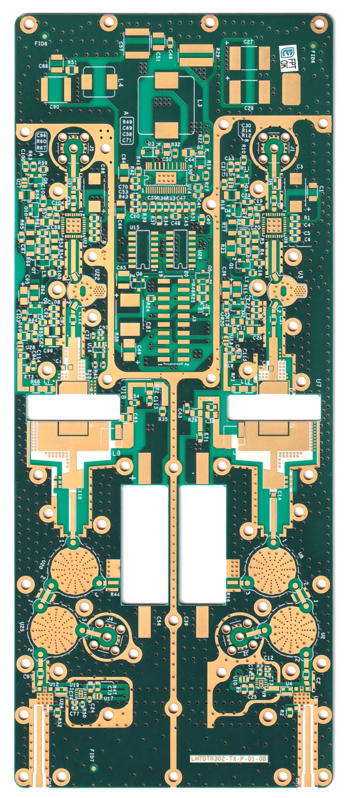
Blind and buried vias fit into a multilayer stack-up when routing density demands it, connecting inner layers without drilling through the whole board. Controlled impedance is held across every layer that carries a high-speed signal, not just the outer ones. Heavy copper layers sit inside the same stack where a board needs to move real current without the extra layers adding thermal risk.
- Blind & buried vias : Inner-layer routing, no wasted drill paths.
- Controlled impedance : Held across the full layer stack.
- Heavy copper layers : Built for current, not just density.
- Mixed substrates: FR4 and Rogers in one stack-up.
- Custom layer maps: Matched to your actual design.
- Engineer-reviewed: Checked before fabrication starts.
One Roof
In-House Multilayer PCB Fabrication Services, Start to Finish
Every stage of your multilayer PCB fabrication happens on our floor, not handed off between vendors. As a multilayer PCB manufacturer in India built for 24-layer output, we hold that same in-house control at volume. No layer’s process step gets outsourced, which means no handoff risk on a build where a single weak step can undo everything above and below it.
Step 1
Drilling
Precision-controlled for every internal layer.
Step 2
Lamination
Pressed and bonded under one process line.
Step 3
Plating
Copper plating done in-house, panel to panel.
Step 4
Testing
Verified before it ever leaves the facility.
Where Layers Go Wrong
Multilayer PCB Manufacturer, Built for 24-Layer Precision
Add a layer to a PCB and you add a new point where registration can shift, where impedance can drift, where a plane can misalign against the one above it. A four-layer board tolerates small errors that a sixteen-layer board can’t hide. By the time you’re at 24 layers, a single misregistered inner layer can take out signal integrity across the whole stack, and that failure won’t show up until the board is already in a system.
Multilayer PCB manufacturing at this depth is not the same discipline as fabricating a two-layer board faster or cheaper. It’s a question of whether the fabricator’s process holds tolerance consistently, layer after layer, on every panel, not just the first one off the line. PC Process runs multilayer PCB manufacturing in Bangalore up to 24 layers, with the layer-to-layer registration control that high-layer-count boards demand, and 43 years of production discipline behind it.
If your board’s reliability depends on what happens between the layers, that’s exactly the part of the process we built around.
Inside the Stack
Inspection That Goes Deeper Than the Outer Layer
AOI Inspection
Catches outer-layer defects before a board moves further down the line.
Fly Probe Testing
Verifies electrical continuity through the full stack, not just top and bottom.
Impedance Measurement
Confirms every high-speed layer performs to spec, inner layers included.
CMI Thickness Checks
Runs per layer, catching copper variance before it reaches the field.
Registration Verification
Confirms inner layers land exactly where the stack-up called for.
100% Coverage
Every board inspected, not a sample batch pulled from the run.
Built for Reliability
Multilayer PCBs for Defence, Aerospace, and Industrial Systems
A multilayer board built for a consumer product and one built for a satellite payload face different consequences when something goes wrong. We build for the second kind. A multilayer PCB manufacturer for aerospace needs LCSO certification under JSS 52302, not just an ISO badge. A multilayer PCB manufacturer for defence electronics needs the same. We hold both.
Defence electronics
LCSO-certified multilayer boards under JSS 52302.
Aerospace & space
High-reliability stack-ups for mission-critical systems.
Medical electronics
Multilayer boards where failure isn't an option.
Telecom infrastructure
Signal-dense builds for high-speed networks.
Industrial automation
Multilayer PCBs built for continuous operation.
Research institutions
Custom stack-ups for specialised applications.
Our Clients
Four Decades of Multilayer PCB Manufacturing, Since 1983






















What is the maximum layer count PC Process can manufacture?
Do you offer multilayer PCB stack-up design support?
Can PC Process manufacture defence-grade multilayer PCBs?
What substrates are available for multilayer PCB fabrication?
Does PC Process manufacture blind and buried via boards?
Can you hold controlled impedance across a full multilayer stack?
Is inspection different for multilayer PCBs compared to standard boards?
Does PC Process manufacture heavy copper multilayer PCBs?
Is all multilayer PCB production done in-house at PC Process?
Which industries does PC Process manufacture multilayer PCBs for?
Stack FAQs

