Blind and Buried Via Boards Manufacturer
Why It Matters
Density Without Compromise
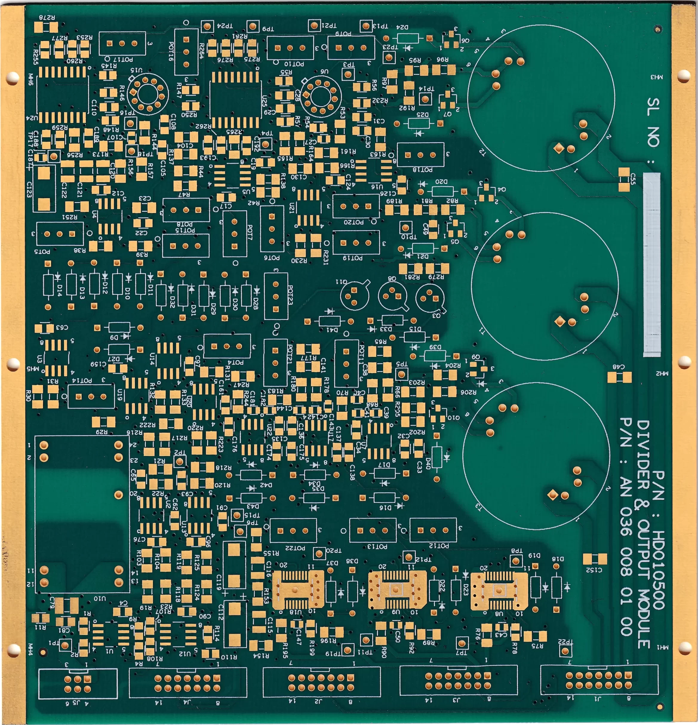
Pack more connections into fewer layers, and the board gets smaller without losing signal integrity. That’s what blind via PCB boards and buried via PCB boards do that standard through-hole construction can’t. For high pin-count BGAs and RF layouts, that density isn’t optional; it’s the only way the design closes.
The gap between a via designed as buried and one manufactured as reliably buried is where boards fail silently. As a Blind and Buried Via PCB manufacturer, PC Process has held that standard since 1983, LCSO certified under JSS 52302, because a via that isn’t fully filled rarely shows up until final test.
Sub-25 Micron Accuracy
100% Inspection
Design Considerations
Getting the Stack-Up Right
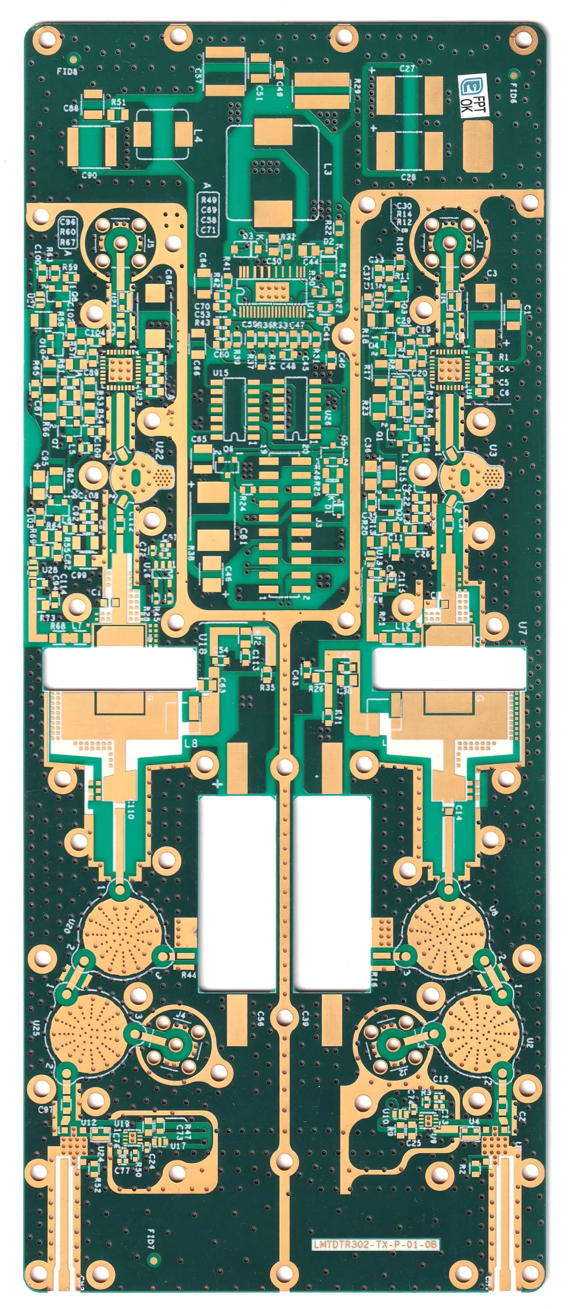
Aspect ratio limits on blind vias and stub length on buried vias aren’t formalities; they determine whether a stack-up is manufacturable as drawn. Layer-to-layer registration tolerance has to be planned into the design stage, not discovered after the first panel runs.
Blind and buried via technology gets specified over standard through-hole approaches when space-constrained multilayer boards, high pin-count BGAs, or RF and high-speed signal paths demand it. Not every stack-up is buried-via-feasible without adjustment, and that’s worth flagging early.
Call it ‘advanced PCB manufacturing’ if you want the label. What it actually means is a stack-up that survives the gap between design intent and what a panel does under lamination pressure.
- Aspect Ratio: Depth-to-diameter limits apply
- Stub Length: Shorter stubs cut signal loss
- Registration: Layer alignment sets tolerance
- Stack-Up Planning: Feasibility decided pre-fab
- BGA Density: Fine-pitch parts need buried vias
- RF Pathways: Shorter paths preserve signal
Production Sequence
From Gerber File to Finished Board
Step 1
Inner Layer Imaging
Inner layers are imaged and etched before any lamination cycle begins, setting the base circuit pattern.
Step 2
Sequential Lamination
Layer pairs are laminated in sequence, with each cycle checked before the next begins to prevent drift.
Step 3
Drilling and Plating
Laser or mechanical drilling per layer pair, followed by plating to form the buried or blind via connection.
Step 4
Outer Imaging and Test
LDI images outer layers, then AOI, fly probe, and CMI checks verify every board before it ships.
Related Capabilities
Often Specified Alongside Blind and Buried Via
Multi-Layer PCB
Up to 24 layers, built for complex, High Density PCB designs.
Controlled Impedance PCB
Signal integrity held to spec for high-speed circuits.
Heavy Copper PCB
Enhanced copper thickness for high-current applications.
FR4 & Rogers PCB
Substrate options suited to RF and standard designs alike.
Custom Blind & Buried Via PCB
Tailored via structures matched to stack-up needs.
Quick Turn PCB
Accelerated timelines without skipped inspection steps.
Manufacturing Precision
Where Registration and Fill Integrity Are Won
Layer-to-layer registration accuracy starts with laser direct imaging, holding sub-25 micron accuracy on outer layers so each buried layer pair aligns exactly where the design calls for it.
Via fill integrity is the harder problem. A void inside a buried via isn’t visible from outside the board, which is why AOI, fly probe testing, and CMI thickness checks run on every unit, not a sample batch.
Blind and buried construction requires sequential lamination, more cycles than a standard Multilayer PCB, and more opportunity for registration drift between each pass. Most generic PCB copy skips this step entirely.
In-house production from DFM to final test keeps registration and fill integrity controlled end to end. There’s no handoff risk between design review and electrical test, because both stages happen under the same roof.
That discipline is why PC Process fabricates for programs, in Bangalore and across India, where a single missed layer pair isn’t something you catch later.
Industries Served
Built for Sectors Where Failure Isn't an Option
Defence
LCSO certified under JSS 52302 for defence-grade traceability.
Aerospace & Space
High-reliability builds for demanding operating environments.
Medical Electronics
Precision boards where signal integrity is non-negotiable.
Telecom & IT
Density and speed for high-throughput communication hardware.
Industrial Automation
Durable boards for continuous operational demands.
Research Institutions
Prototype-to-production support for R&D programs.
Why PC Process
Certified, Traceable, Proven
- ISO 9001:2015 and LCSO Certified: Quality management and defence-grade traceability under JSS 52302, verified standards a specification sheet alone can't claim.
- 43+ Years in Fabrication: Since 1983, blind and buried via construction has run under the same in-house discipline, not outsourced at any stage.
- Trusted by ISRO, HAL, and BEL: High-reliability sectors have specified PC Process boards for programs where failure isn't recoverable after the fact.
- 100% In-House, 100% Inspected: DFM to final test under one roof, with every board inspected, not sampled, before it ships.
Client Feedback
What Engineers Say
Our Clients
Trusted Across High-Reliability Sectors






















What's the difference between a blind via and a buried via?
What aspect ratio limits apply to blind via designs?
How is via fill integrity verified if it isn't visible externally?
Can blind and buried vias combine with controlled impedance requirements?
Is blind and buried via construction available for prototype quantities?
How does sequential lamination affect blind and buried via reliability?
Is blind and buried via technology the same as HDI PCB design?
What substrates are available for blind and buried via boards?
Does PC Process review the Gerber file before quoting a blind and buried via board?
Is PC Process a blind and buried via boards manufacturer for both prototype and production runs?
Frequently Asked