
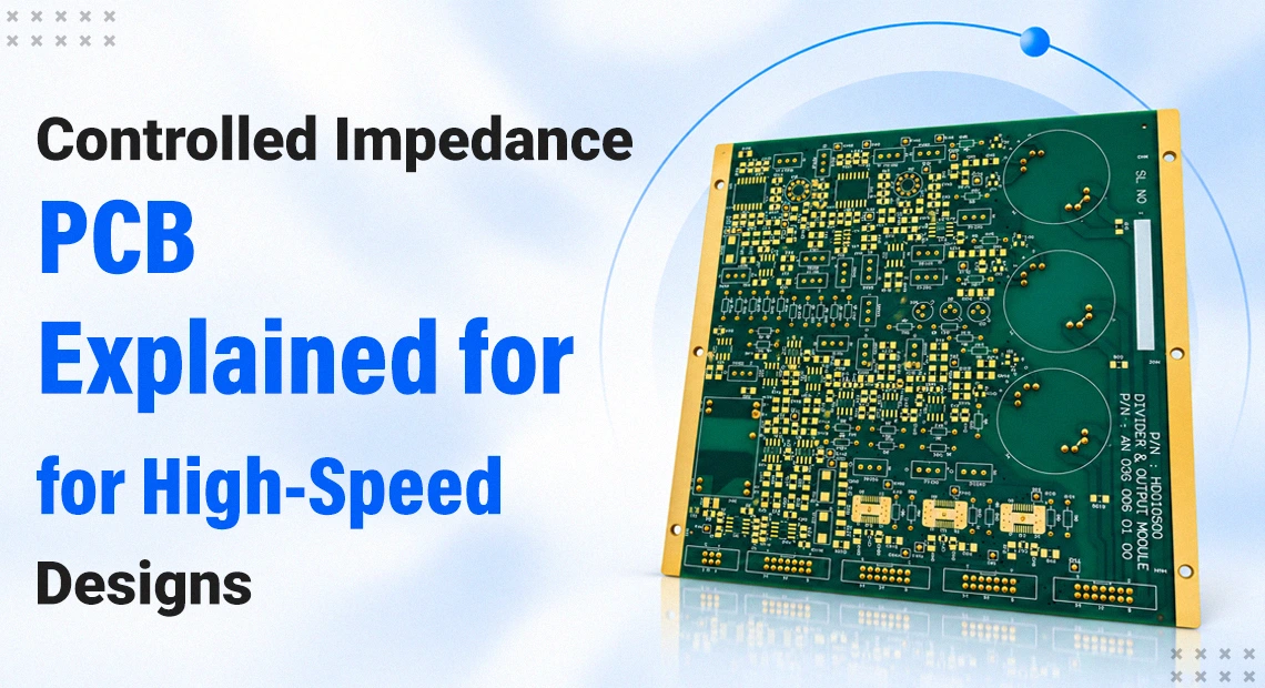
A schematic shows which pins connect. The board decides how the signal actually travels between them. On fast digital and radio-frequency designs, that journey depends on the physical structure of the board, and controlled impedance PCB manufacturing is the discipline that keeps it predictable. This guide explains the concept, the design choices that shape it and the manufacturing steps that protect it.
What is controlled impedance in PCBs?
Impedance is the opposition a trace presents to a changing signal. It depends on the width of the trace, the thickness of copper, the insulating material around it and the distance to the nearest reference plane.
A controlled impedance PCB is built so that these factors are held within an agreed range. The designer specifies a target for chosen traces, and the manufacturer builds the board to meet it, then verifies the result.
Why impedance control is needed in high-speed PCBs
When a signal changes state quickly, the trace behaves like a transmission line. Any change in impedance along the path reflects part of the signal back towards its source. The outcomes are ringing, distorted edges, timing errors and noise that spreads to neighbouring circuits.
High-speed PCB impedance control keeps the path uniform so the receiver sees the signal the driver sent. The need grows with faster edge rates, longer traces and tighter timing budgets. It applies to high-speed digital buses, differential pairs, clock lines and every high-frequency PCB that carries radio or microwave signals.
Microstrip vs stripline impedance
Both structures are transmission lines. They differ in where the trace sits in the board.
| Microstrip | Stripline | |
| Location | Outer layer | Inner layer |
| Reference | One plane below | Planes above and below |
| Shielding | Exposed to air and surface finish | Enclosed by planes |
| Typical use | Short, accessible RF routing | Dense, noise-sensitive routing |
Microstrip is easier to probe and rework, and the surface finish and solder mask influence its behaviour. Stripline offers better isolation from outside interference, and its impedance is governed almost entirely by the dielectric layers around it. Many designs use both, which makes the stack-up a shared decision between designer and manufacturer.
How stack-up affects impedance
The stack-up is the ordered arrangement of copper layers and insulating layers. It sets the distance between each signal trace and its reference plane, and that distance is one of the strongest influences on impedance.
A controlled impedance PCB stack-up involves several linked choices:
- Dielectric thickness between signal and reference layers
- Material type and its dielectric constant
- Trace width and copper weight on each layer
- Reference plane arrangement, including how return paths are provided
Changing any one of these shifts the others. For that reason the best results come from agreeing the stack-up with the manufacturer before layout is finalised, because the manufacturer knows which laminates and prepregs are available and how they behave after pressing.
FR4 vs Rogers for impedance control
FR4 is the established general-purpose laminate. It suits a wide range of digital designs and offers good value, and many high-speed boards perform well on it when the stack-up is planned carefully.
Rogers laminates are engineered for applications where dielectric properties must stay stable across frequency and temperature, and where signal loss must be kept low. That makes them the usual choice for RF, microwave and other high-frequency work. Some designs combine both: Rogers on the layers carrying critical signals and FR4 elsewhere, which balances performance and cost.
The choice follows the operating frequency, the loss budget and the environment the board will face.
Where impedance control is decided in manufacturing
Design intent only becomes a working board if the manufacturing process holds to it. Four stages carry most of the responsibility.
Design review
An engineering review of the Gerber data and the requested stack-up checks that the target impedance can be achieved with available materials and the proposed trace geometry. Adjustments are agreed with the designer at this point, when changes are simple.
Imaging and etching
Trace width has a direct effect on impedance, so the accuracy of imaging matters. PC Process uses Laser Direct Imaging, which removes film registration errors and gives precise control of outer layer features. Etching is then compensated so the finished trace width matches the calculated one.
Lamination
Pressing determines the final dielectric thickness between layers. Controlled lamination and layer registration keep the dielectric consistent from one board to the next.
Inspection and measurement
PC process applies 100% inspection to every board. This includes AOI, flying probe testing, thickness checks with CMI equipment and impedance measurement. Every unit is verified individually, and all of it takes place in-house from review through to final test, which gives full traceability.
How PCB impedance is measured
Impedance is commonly measured with a time-domain reflectometer. The instrument sends a fast pulse down the trace and analyses the reflections to calculate impedance along its length.
Measurements are taken on the board itself or on dedicated test coupons built into the production panel. Coupons are designed to represent the controlled traces and allow checking without affecting the working circuit. The result confirms that the board matches the specified target within the agreed tolerance.
Controlled impedance PCB manufacturer in India
Choosing a controlled impedance PCB manufacturer in India or Bangalore comes down to process control, verification and engineering support during design. PC Process has manufactured prototype and low-volume multi-layer boards from Peenya, Bangalore, since 1983 and holds ISO 9001:2015 certification and LCSO certification under JSS 52302. Our customers include design teams in aerospace, defence, telecom, medical electronics, and industrial automation.
Learn more about our controlled impedance PCB manufacturing capabilities and multi-layer PCB services or share your stack-up and impedance requirements with our engineers. Contact our team to discuss your project or request a quote.
Frequently asked questions
1. What is controlled impedance in a PCB?
Controlled impedance means the characteristic impedance of selected traces is designed, manufactured and verified to fall within an agreed range. It depends on trace width, copper thickness, the dielectric material and the distance to the reference plane. The designer sets the target, and the manufacturer builds and tests the board to match it.
2. Why is impedance control important in high-speed PCB design?
At fast edge rates, a trace behaves as a transmission line, and any impedance change along it reflects part of the signal back towards the source. That distorts edges and adds timing errors and noise. Impedance control keeps the path uniform from driver to receiver, which protects signal integrity as speeds rise.
3. What happens if a PCB does not have controlled impedance?
Reflections at impedance mismatches cause ringing, overshoot, data errors and noise coupling into neighbouring circuits. These faults often appear only at full operating speed, so a board can pass basic continuity checks and still fail during validation.
4. What is the difference between microstrip and stripline?
Microstrip traces run on an outer layer with one reference plane beneath them. Stripline traces run on an inner layer between two reference planes. Microstrip is easier to probe and rework, while stripline offers better isolation from outside interference. Many boards use both.
5. How does PCB stack-up affect impedance?
The stack-up sets the dielectric material and the spacing between each trace and its reference plane. Combined with trace width and copper weight, these values determine impedance. A change in dielectric thickness or material shifts impedance for the same trace width, so stack-up and trace widths should be settled together with the manufacturer before layout.
6. How is PCB impedance measured?
A time-domain reflectometer sends a fast pulse down a trace and reads the reflections to calculate impedance. Measurement is made on the board or on test coupons built into the production panel. The result is compared with the target set for each controlled trace.
7. What is the standard impedance tolerance for a PCB?
No single tolerance applies to every board. The tolerance is set by the application and written on the fabrication drawing. Tighter tolerances demand closer control of trace width, dielectric thickness and material consistency, and the range a manufacturer can hold depends on its process and the laminate chosen. Ask for the achievable tolerance before finalising layout.
8. Can FR4 be used for controlled impedance PCBs, or is Rogers required?
FR4 works for many controlled impedance designs, particularly digital ones, when the stack-up is planned carefully. Rogers laminates suit RF, microwave and other high-frequency designs that need stable dielectric properties and low signal loss. Some boards combine both, with Rogers on critical signal layers and FR4 elsewhere.
9. What information should I send a manufacturer for a controlled impedance PCB?
Send the Gerber files, the target impedance for each controlled net, trace type (single-ended or differential), preferre


