PCB for Power and Energy Applications
Specification Priorities
What a Power PCB Manufacturer Must Get Right
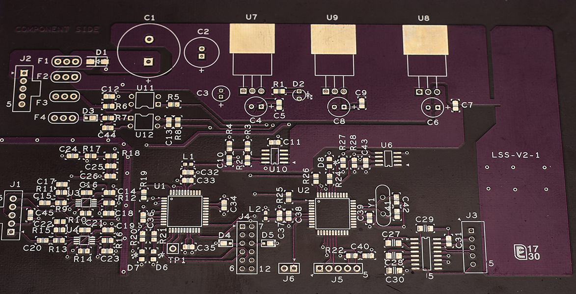
Copper weight, dielectric spacing and thermal paths decide how long a power board runs under load. A 28.35-gram (1 oz) copper layer is about 35 µm thick, and each added ounce raises the current a trace carries at a given temperature rise.
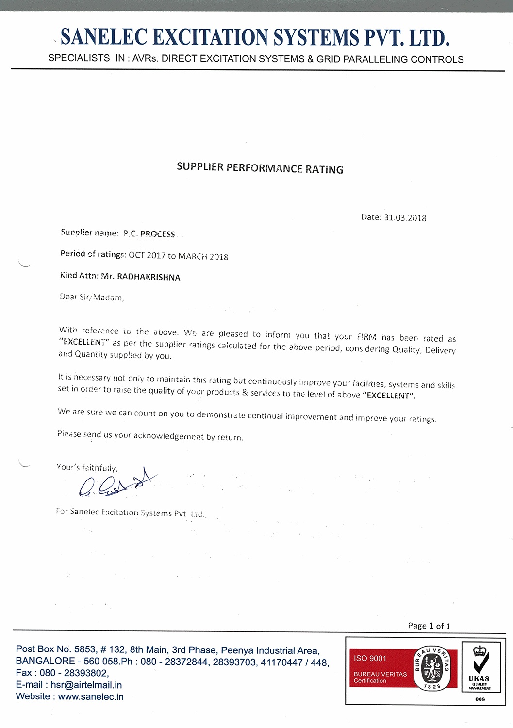
A PCB for power and energy applications is judged on the copper weight a manufacturer can process, the laminate it stocks and the depth of its inspection. PC Process has manufactured in-house since 1983 and checks every unit it ships.
- Copper weight matched to the current each trace carries
- Laminate with a glass transition temperature suited to sustained heat
- Via structures that carry current and conduct heat
- Spacing set for the working voltage
- ENIG or HASL finish chosen for the storage and soldering route
- Electrical test on every board before dispatch
Core Use Cases
Six Applications Where Copper Weight Decides Performance
These six applications carry the highest currents, voltages and thermal loads in energy systems, and each depends on copper, insulation and heat paths controlled in-house at PC Process.
Energy Storage
Storage racks cycle high current through wide copper pours. Heavy copper layers keep resistive heating low during every charge and discharge cycle.
Battery Management Systems
Cell monitoring boards pair low-voltage sense lines with high current paths. Controlled spacing keeps the two domains isolated across the board.
High Voltage Control
Control boards at high voltage need clearance and creepage set for the working voltage. Laminate and finish follow from that spacing and the environment.
Voltage Converters
Converter stages switch large currents at high frequency. Heavy copper and thermal vias move heat out of switching devices and nearby magnetics.
Power Factor Correctors
PFC stages combine inductors, switches and sense circuits on one board. Copper weight and layout set the thermal margin when the stage runs at full load.
Wind Energy Systems
Pitch, converter and control boards work through vibration and wide temperature swings. Board material and finish are chosen for that duty cycle.
Role in the System
Why Energy Systems Depend on Power Conversion Boards
Solar, wind, hydropower and storage sites move power through chains of boards. Six functions explain why board quality sets the reliability of the whole installation, from converters to controls.
Efficient Power Conversion
Converters in smart grids and solar inverters switch large currents continuously. Low-resistance copper paths cut conduction loss and reduce the heat the board must shed to the enclosure.
Tough Conditions
Hydropower stations and outdoor enclosures expose boards to humidity, heat and vibration. Laminate selection and surface finish decide how long the board holds up in that environment.
Compact and Lightweight Design
Heavy copper lets one board carry power and control circuits together, which shortens interconnects, cuts harness length and saves enclosure space in compact converters and storage units.
Safety First
Insulation spacing, defined fault paths and tested continuity protect equipment and the people around it. Fly probe testing runs on every board we ship, so each unit is electrically verified.
Engineering Inputs
Design Considerations for High Power PCBs
A high power PCB starts with a thermal budget. Engineers set it from the current each net carries and the temperature rise the enclosure allows, then choose copper weight, laminate and via count to meet it.
Thermal management reaches beyond the board. Component placement, heatsink contact and enclosure airflow all change how much current a copper weight can carry. Sharing these inputs at the DFM stage lets us settle stack-up before production.
- Airflow: Airflow direction and heatsink contact decide where copper area and thermal relief are placed.
- Amount of power: Total load and peak current set copper weight and trace width.
- Board material: Laminate Tg and thermal conductivity govern sustained heat. FR4 and Rogers are both available.
- Temperature: The allowed temperature rise sets conductor cross-section, and IPC-2152 charts guide that sizing.
- Vias: Via count and plating thickness set the current an array carries; CMI checks confirm plating on every unit.
Failure Modes
Challenges of High Current PCBs
Durability depends on how copper, laminate and plating behave across thousands of thermal cycles. Via barrel plating is a known crack site under that stress, so CMI thickness checks measure it on every unit we ship.
Failsafes belong in the layout: fuse locations, wide spacing around protected nets and defined current paths. Temperature is the third variable, because a board that runs hot ages faster. Thermal margin is built in from the first stack-up.
Compliance Context
Ruggedisation and Regulatory Standards for Power Boards
Ruggedisation covers laminate choice, ENIG or HASL finish, coating compatibility and mechanical support for heavy components. Energy equipment also carries product-level regulation, which the board design has to support.
Our quality system is ISO 9001:2015 and LCSO certified under JSS 52302, the Indian defence supplier standard. The references below guide power board design, and product approval stays with the equipment maker who certifies the finished system.
- IPC-2221: Common rules for conductor spacing and board design.
- IPC-2152: Current carrying capacity of printed board conductors.
- IEC 60664-1: Insulation coordination, clearance and creepage.
- IEC 62477-1: Safety requirements for power electronic converters.
- IEC 62109-1: Safety of power converters in photovoltaic systems.
Industry Footprint
Where High Current Boards Are Used
Eight equipment groups use high current boards, from EV chargers and solar parks to welding sets and transformer control units, each with its own mix of copper, spacing and thermal needs.
Automotive
EV charger boards, onboard converters and battery systems carry high current in a compact footprint under vibration and heat.
Aviation
Power distribution and conversion boards for aerospace equipment need consistent copper weight and verified plating.
Heavy Machinery
Motor drives and control boards work through vibration, heat and sustained high current loads on factory floors.
Power Converters
PCBs for power conversion use heavy copper for low conduction loss and for spreading heat from switches.
Power Supplies
A PCB for power supply and control systems pairs high current outputs with precise sense and feedback circuits.
Solar Arrays
String combiners, inverters and PCBs for solar panel parks carry high DC current outdoors, year after year.
Transformers
PCBs for transformer control hold sensing and protection circuits beside high current paths and insulation barriers.
Welding
Welding equipment pulses very high current, so copper weight and plating quality set the life of the board.
Production Route
From DFM Review to Final Test Under One Roof
Step 1
In-House DFM Review
Engineers check stack-up, copper weight and conductor spacing against your Gerber files before any production step starts.
Step 2
Laser Direct Imaging
LDI removes film registration error and holds sub-25 µm accuracy on outer layers, so fine sense lines stay aligned.
Step 3
Optical and Electrical Testing
AOI checks circuit patterns, fly probe testing verifies continuity and isolation, and impedance is measured on every unit.
Step 4
CMI Thickness Checks
CMI checks measure copper and plating thickness on every board, confirming the current-carrying cross-section.
Trusted Since 1983
Organisations We Manufacture Boards For






















Direct From Customers
Feedback From Teams That Build With PC Process
What is a power PCB?
What is a heavy copper PCB manufacturer?
How much current can a PCB trace carry?
Which materials suit high power boards?
How does a high voltage PCB manufacturer set spacing?
Is PC Process an EV charger PCB manufacturer?
What order sizes does a power conversion PCB manufacturer handle?
How does the DFM review work?
Which sectors does a power electronics PCB manufacturer like PC Process serve?
Which certifications does PC Process hold?
Common Questions