
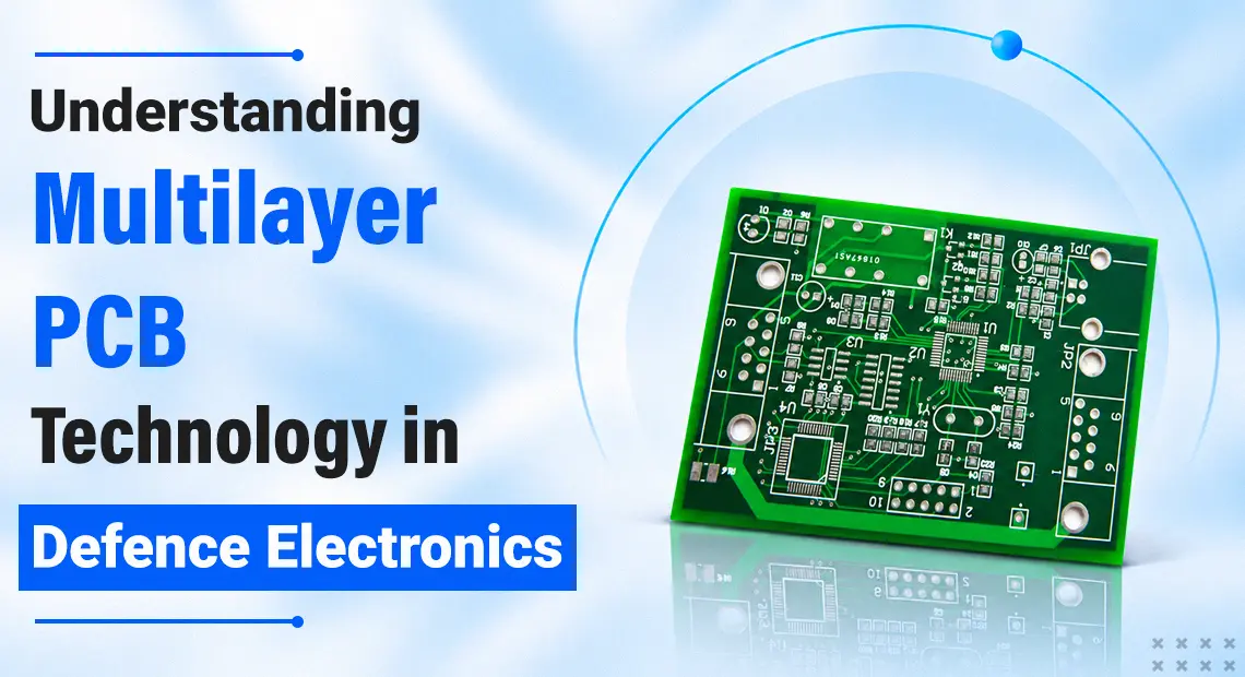
Multilayer printed circuit boards play an important role in modern defence electronics, supporting the complex circuits used in radar systems, avionics, secure communication equipment and ground stations. Their layered construction allows multiple electrical functions to operate within a compact board while maintaining signal integrity, power distribution and circuit isolation. Understanding how these boards are structured, which materials are used and what quality standards apply helps explain their importance in defence applications.
Quick answer. A multilayer PCB for defence electronics stacks alternating copper and dielectric layers, with dedicated power and ground planes and controlled-impedance signal layers. It is built to a high-reliability class and verified through full inspection. High-Tg FR4 serves the digital and power layers, and Rogers laminates serve the RF layers. In India the reference document is JSS 52302, and suppliers hold LCSO approval to build on it.
Why defence electronics need multilayer PCBs
Airborne and portable platforms limit board size and weight, while the circuits inside combine high-speed digital, power and RF sections. Four properties of multilayer construction address this:
- Density: extra routing layers fit the same function into a smaller footprint.
- Power integrity: solid planes give low-impedance current paths and a clean return for every signal.
- Signal integrity: inner signal layers referenced to adjacent planes allow controlled impedance for high-speed and RF lines.
- Isolation: inner ground planes separate sensitive receiver circuits from noisy switching sections.
Layer count in defence boards
Layer count follows function and density. Power and interface cards sit at the low end. Processing boards with BGA escape routing sit higher, and RF front ends add low-loss layers and shielding planes. Designers who search for a 24-layer PCB manufacturer in India are typically matching a dense processing card or hybrid RF board to a stated capability; PC Process, for example, manufactures up to 24 layers.
More layers tighten cumulative registration, and each sequential lamination cycle used for blind or buried vias adds further tolerance. The right count is therefore the lowest one that closes the routing and plane requirements. Laser Direct Imaging removes film registration error from the outer-layer imaging step.
Multilayer PCB stack-up for high reliability
A high reliability multilayer PCB matches each layer’s material to its job: high-Tg FR4 for digital and power layers, Rogers laminates where RF loss matters, and a symmetrical build to limit bow and twist.
Laminates for defence boards
In a hybrid stack-up, Rogers cores carry the RF layers while FR4 prepreg bonds them into the rest of the board. Polyimide suits higher-temperature designs. An unbalanced build can warp during lamination and later soldering, so materials are placed symmetrically about the centre line. The FR4 and Rogers PCB page lists laminate options.
RF multilayer PCB for radar and communication
An RF multilayer PCB for radar and communication keeps RF signals on low-loss layers, with FR4 carrying the digital and power circuits. Impedance targets set dielectric thickness and trace width, so they are fixed in the stack-up before layout freezes. Controlled impedance PCB manufacturing covers impedance control in more detail.
Blind and buried vias in radar boards
Blind vias connect an outer layer to the nearest inner layers, and buried vias connect inner layers only. On radar boards they shorten vertical transitions and release outer-layer space. Through-hole vias leave stubs that resonate at millimetre-wave frequencies, and blind vias remove them. Each via type adds drilling and lamination steps, so the structure is settled at stack-up stage. The blind and buried via boards page describes the construction.
JSS 52302, LCSO and MIL-PRF-31032 explained
JSS 52302 is India’s joint service specification for multilayer, through-hole bare boards, and its 2024 fourth revision was developed with ISRO, CEMILAC, BEL, ECIL and IPC. The JSS 52302 PCB standard is the document an Indian defence drawing names when it calls for these boards.
LCSO is the approval a manufacturer holds to supply to that specification. Indian multilayer manufacturers list LCSO approval alongside JSS compliance. An LCSO certified PCB manufacturer holds it for a stated scope, and defence supplier directories list LCSO approved PCB manufacturers in India. MIL-PRF-31032 is the US performance specification, tied to a DLA qualified manufacturers list.
| Item | JSS 52302 | MIL-PRF-31032 | IPC-6012 Class 3 |
| Origin | Indian defence joint service specification | US Department of Defense performance specification | IPC industry standard |
| Board scope | Multilayer, through-hole bare boards | All PCB types | Board qualification and performance |
| Qualification route | LCSO approval of the manufacturer | DLA qualified manufacturers list | Called out on the drawing or order |
IPC Class 3 requirements and military-grade boards
IPC Class 3 PCB requirements are the strictest acceptance criteria in IPC-6012, written for boards that must perform on demand. Military grade adds a performance specification, qualified materials and traceability on top of that class. A military PCB manufacturer, in the usual sense of the term, is a supplier qualified to JSS 52302 for Indian programmes or MIL-PRF-31032 for US programmes. The specification called out on the board’s drawing settles which of the two governs.
What supplier credentials mean
Five checks turn credentials into evidence:
- Certificate scope: The LCSO or ISO certificate lists the specification, layer count and technology it covers, and its validity dates.
- Production control: Imaging, plating, lamination and test each add a handoff to traceability when they run outside the plant.
- Inspection coverage: Sampling and inspecting every unit give different assurance. AOI, fly probe testing, impedance measurement and thickness checks are the usual methods.
- Design review: A stack-up and via structure review before release catches registration and impedance issues early.
- Prototype route: A prototype multilayer PCB for defence built on the same line as the production run keeps the qualified process unchanged.
The checks apply to any multilayer PCB manufacturer in India buyers compare, including the indigenous PCB manufacturers for defence that supply domestic programmes and the multilayer PCB manufacturers in Bengaluru, where PC Process operates from Peenya.
Common mistakes: freezing the layout before the stack-up is agreed; naming a specification the supplier does not hold; building an unbalanced material stack; leaving impedance targets off the drawing notes.
Where defence multilayer boards are heading
Domestic standards such as JSS 52302 are becoming the reference for Indian programmes; via structures and feature sizes, they tighten as processors densify; and radar and communication boards carry more hybrid RF construction.
Key takeaways: Choose the lowest layer count that closes the design, and keep the stack-up symmetrical. Match the supplier’s certificate to the specification on the drawing.
Founded in 1983, PC Process is a defence PCB manufacturer in India that supplies customers including HAL, BEL and ISRO (through VSSC). Engineers with a specific board can discuss PCB requirements with the team, and the multilayer PCB manufacturing page lists capability details.
Frequently asked questions
1. What is a multilayer PCB used for in defence electronics?
They host the circuitry of radar, avionics, secure radios and ground equipment, combining dense routing with solid power planes and controlled impedance on one board.
2. Why do defence electronics need multilayer PCBs?
Platforms limit size and weight, so more circuitry must fit on less board. The layer structure supplies dedicated planes, controlled impedance and isolation between RF, digital and power sections.
3. How many layers does a defence PCB have?
It depends on function and density. Interface cards need fewer layers, while processing and RF boards need more. PC Process manufactures multilayer boards up to 24 layers.
4. What is JSS 52302?
JSS 52302 is India’s joint service specification for multilayer, through-hole bare boards, revised in 2024 with ISRO, CEMILAC, BEL, ECIL and IPC.
5. What is LCSO certification for PCB?
LCSO is the Indian defence approval that lets a manufacturer build multilayer boards to joint service specifications. Buyers check its scope and validity dates.
6. JSS 52302 vs MIL-PRF-31032: which applies to a board?
JSS 52302 is the Indian specification, backed by LCSO approval. MIL-PRF-31032 is the US specification, tied to a DLA qualified manufacturers list. The drawing names the one that applies.
7. IPC Class 3 vs. military-grade PCB: what separates them?
IPC Class 3 is a reliability class for boards that must work on demand. Military grade adds a performance specification, qualified materials and traceability on top of that class.
8. How are blind and buried vias used in radar boards?
Blind vias join an outer RF layer to the nearest inner plane, and buried vias join inner layers. Both shorten vertical transitions, remove stubs and free surface space.
9. What laminate is used for defence PCBs?
High-Tg FR4 for digital and power layers, Rogers or PTFE laminates for RF layers, often bonded with FR4 prepreg in a hybrid stack-up. Polyimide serves higher-temperature designs.
10. How to choose a defence PCB manufacturer?
Match the certificate scope to the specification and layer count, confirm where each process step runs, ask whether every unit is inspected, and request a stack-up review before release.


