
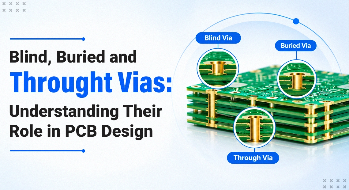
On a multilayer board, a via is drilled and plated early, then hidden beneath pressed layers and a solder mask. By the time a board reaches electrical test, the decisions behind each of these plated holes were made earlier in the stack-up, and revisiting them means a new build.
Blind and buried vias in PCB designs take shape at separate stages of the build, and that timing sets the manufacturing route. Buried types are drilled and plated on inner cores before final lamination; blind ones are drilled from an outer layer to a set depth, and full-depth holes are drilled after the stack is pressed. Aspect ratio, lamination cycles and registration decide whether the structure can be built reliably.
PCB via types compared
A through-hole via vs. a blind via vs. a buried via comparison comes down to the layers each connects and when it is formed.
| Type | Connects | Formed | Manufacturing consequence |
| Through | Every layer | After final lamination | Simplest route; leaves a barrel stub on high-speed nets |
| Blind | Outer layer to inner layers | Controlled-depth or laser drilling | Depth control and aspect ratio limits |
| Buried | Inner layers only | Before final lamination | Sealed in after pressing; cannot be reworked |
| Microvia | Adjacent layers | Laser drilling on build-up layers | Tight aspect ratio; fill choices matter |
In a blind via vs buried via choice, the blind option frees routing space under fine-pitch packages from the board surface. The buried option keeps interlayer connections off the outer layers and leaves surface area for components.
How are blind and buried vias manufactured?
The route follows the stack-up, but a typical sequence looks like this:
- Core preparation. Inner layers are imaged and etched, and cores that carry buried connections are drilled and plated before lamination around them.
- Sequential lamination. Layers carrying these connections are pressed together and drilled, and further layers are added afterwards.
- Blind-hole formation. Laser ablation forms microvias, and controlled-depth mechanical drilling forms larger blind holes. Each stops on its target copper pad.
- Plating, fill and finish. Copper is plated down each barrel, holes under component pads are filled and capped, and the board is finished in ENIG or HASL and electrically tested.
How many lamination cycles does a buried via need?
The count depends on where the structure sits in the stack-up. A buried connection inside a single core is drilled and plated on that core, so the board still sees only its final press. One spanning several cores, or sitting inside a sub-stack, needs that sub-stack laminated first. That adds a press cycle, and each further level of nesting adds another.
How high can a blind via aspect ratio go?
Aspect ratio is depth divided by drilled diameter, and it decides whether copper plates are evenly down the barrel. Full-depth holes tolerate a much higher ratio than blind ones, and laser microvias are held shallow relative to their diameter. Industry standards set a ceiling, and each manufacturer states its own blind via aspect ratio limit within it. For a given limit, a deeper blind hole needs a larger drilled diameter, which consumes routing area.
Why do blind and buried vias increase PCB cost?
Blind and buried via cost rises because each structure adds work that a plain through-hole build avoids:
- Extra press cycles, each with pressing, curing and re-registration.
- Separate drill and plating passes for each structure.
- Yield exposure, because a defect in a buried layer is sealed in once pressed.
- Tighter material and registration control across repeated thermal cycles.
Published uplift figures vary widely by structure and stack-up, so a quote on the actual design is the reliable number.
Microvia vs blind via, and HDI
A microvia is a laser-drilled blind or buried hole, usually spanning one dielectric layer. Blind via is the wider class, and microvia is its smallest form. Stacks that grow stage by stage from a central core are where HDI blind and buried vias typically appear. The line between an HDI PCB and a standard multilayer PCB follows from this: HDI combines microvias with build-up layers, while a standard multilayer board relies mainly on full-depth holes.
Choosing Blind Vias Over Through-Hole Vias at the Stack-Up Stage
Run a press count check before committing a stack-up:
- Density: Escape routing under fine-pitch BGAs and via-in-pad placement are the usual reasons to go blind.
- Aspect ratio: Divide depth by diameter and compare with the manufacturer’s limit.
- Sub-stacks: Each one adds a press, cost and lead time.
- Signal integrity: A full-depth hole leaves an unused stub, and combining blind or buried connections with it removes the stubs.
If a full-depth hole routes the net, it carries the lowest process risk. A few blind connections that solve a specific escape problem are usually worth the added steps.
Checklist before release
- Define every span: Blind holes sit in a separate drill file, so the drill chart must state start and stop layers.
- Specify fill and cap: Pad-mounted holes must be filled and capped, or solder wicks into the hole and starves the joint.
- Stagger where possible: Standards guidance recommends staggering for complex HDI.
- Inspect inner layers before pressing, since buried layers cannot be checked afterwards.
Blind and buried via PCB capability at PC Process
PC Process manufactures prototype and low-volume multi-layer PCBs in Peenya, Bengaluru, with blind and buried via boards within its multi-layer range. Production runs in-house from DFM review to final test, so the interconnect structure is discussed with the engineers who build the board. Laser direct imaging removes film registration error on outer layers, and every unit is inspected with AOI, fly probe testing, impedance measurement and CMI thickness checks. The company is ISO certified and LCSO certified under the Indian defence supplier standard, serving aerospace, defence, telecom, medical electronics, automotive and industrial automation.
Conclusion
Interconnect structure is a manufacturing decision as much as a routing one. Use full-depth holes where they route the net and blind connections where density demands them, and treat every sub-stack as a cost and lead time decision.
Discuss your blind and buried via requirements with the PC Process team. Request a quote, and our engineers will review your stack-up as part of a free DFM review.
Frequently Asked Questions
1. What are blind and buried vias in a PCB?
A blind via links an outer layer to inner layers. It is buried via links in inner layers only and stays hidden from both surfaces. Both need extra drilling and lamination steps compared with a full-depth hole.
2. How are blind and buried vias manufactured?
Buried connections are drilled and plated on a core before final lamination. Blind holes are formed by laser or controlled-depth drilling from an outer layer, then plated and often filled.
3. What is the difference between a blind via and a buried via?
A blind via opens to one outer surface and ends at an inner layer. A buried via sits entirely between inner layers, so it is sealed in during pressing and cannot be reworked afterwards.
4. What is the maximum aspect ratio for a blind via?
Aspect ratio is depth divided by drilled diameter, and each manufacturer sets its own limit from its plating capability. Confirm that limit early, before the stack-up is fixed.
5. Why do blind and buried vias increase PCB cost?
They add press cycles, separate drilling and plating passes, and tighter registration control. A defect in a buried layer is sealed in after pressing, which raises yield risk.
6. How many lamination cycles does a buried via need?
A buried connection inside one core needs only the final press. One spanning several cores or a sub-stack needs that sub-stack laminated first, adding a press per level of nesting.
7. When should I choose blind vias over through-hole vias?
Choose blind construction when density, such as BGA escape or via-in-pad placement, requires it and the aspect ratio holds. Otherwise, a full-depth hole carries lower process risk.
8. What is the difference between a microvia and a blind via?
A microvia is a laser-drilled blind or buried hole, usually one dielectric layer deep. Blind via is the wider class, and microvia is its smallest form, found mainly in HDI boards with build-up layers.
9. How does an HDI PCB differ from a standard multilayer PCB?
HDI boards combine microvias with build-up layers added in stages. A standard multilayer board relies mainly on full-depth holes, adding blind or buried connections only where density demands.
10. Does the PC process manufacture blind and buried via PCBs?
Yes. Blind and buried via boards are part of its multi-layer range, built in-house with a free DFM review. Request a quote, and the engineers will check feasibility against your stack-up.


