
Design & Planning
Layer Processing & Fabrication
Testing & Quality Control
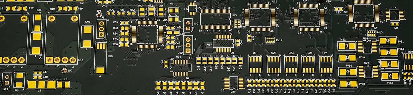
Fully in-house production
No outsourcing at any stage. Every process from DFM to final test happens under one roof, giving you complete traceability and zero handoff risk.
End-to-end quality control
AOI, fly probe testing, impedance measurement, and CMI thickness checks are applied to every board not sampled, but every unit.
Laser-precision imaging
Laser Direct Imaging eliminates film registration errors, delivering sub-25 µm accuracy on outer layers and consistent yields on tight-pitch designs.
Environmentally responsible
Our on-site reverse osmosis wastewater treatment plant ensures full regulatory compliance and responsible discharge meeting the highest environmental standards.
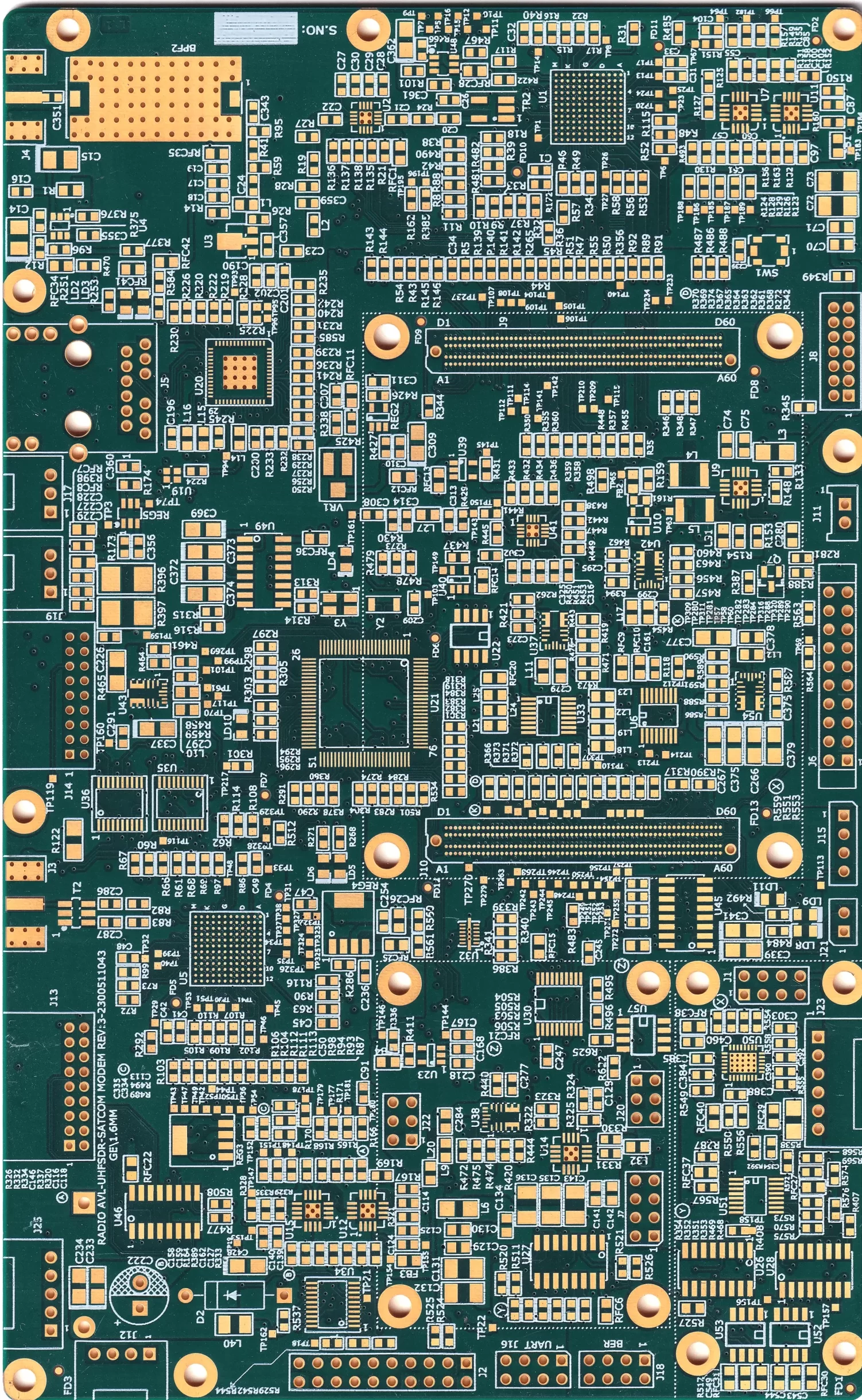
Ready to start your next build?
Upload your Gerber files for a free DFM review and instant quotation. Our engineers respond within 2 hours.

