
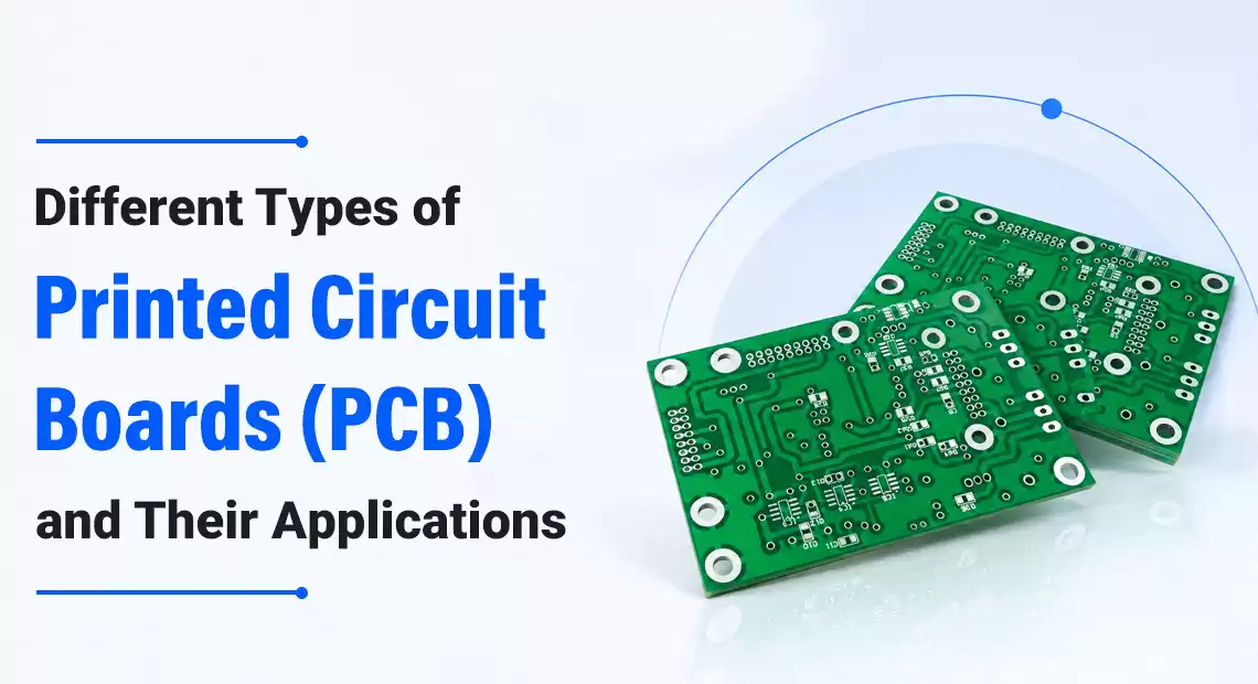
A printed circuit board is a laminated structure of conductive copper traces and insulating substrate that mechanically supports and electrically connects electronic components.
PCBs fall into a few structural categories: single-sided, double-sided, multilayer, rigid, flexible, rigid-flex, and HDI. The right type depends on routing complexity, current or signal speed, and the environment the finished product will operate in.
This page draws on 43+ years of PCB fabrication experience across defence, aerospace, medical, and telecom applications, including in-house production from prototype through to volume.
Why PCB Type Selection Isn’t Just a Cost Decision
Most explanations treat PCB type as a budget question: single-sided is cheap, multilayer is expensive. That framing misses the engineering reality: board type determines signal integrity, thermal behaviour, and long-term reliability under real-world stress.
In defence or medical electronics, an unsuitable board design can create serious reliability risks in the field. The real question isn’t which PCB type is cheapest. It’s which type matches the electrical, thermal, and mechanical demands of where the board will actually operate.
Types of PCB by Construction
Single-Sided PCBs
One copper layer on one face of the substrate. Lowest cost, simplest to fabricate. Used in: calculators, basic power supplies, LED drivers, simple sensor circuits. Routing density is capped; complex designs outgrow it quickly.
Double-Sided PCBs
Copper on both sides, connected by plated vias. More layout complexity than single-sided, without multilayer’s tight registration demands. Used in industrial control panels, automotive instrument clusters, amplifiers, and power monitoring systems.
Multilayer PCBs
Three or more conductive layers are separated by dielectric and interconnected by vias, typically 4 to 24+ layers. PC Process’s in-house multilayer capability runs up to 24 layers. Used in: satellite electronics, avionics, medical imaging, telecommunication infrastructure, and defence communication systems.
Expert insight: layer count alone doesn’t determine board quality. Two 12-layer boards can perform very differently depending on stack-up design and how tightly registration is controlled during lamination.
Rigid PCBs
A stiff substrate, most commonly FR4 fibreglass-epoxy, that holds its shape permanently. The default construction for most electronic products. Used in motherboards, telecommunications equipment, industrial controllers, and ground-based defence systems.
Flexible PCBs
Bendable substrates, typically polyimide, that twist, fold, or conform to non-flat spaces, reducing connector and cabling weight. Used in: wearable medical devices, foldable electronics, automotive sensor arrays, camera modules.
Rigid-Flex PCBs
Rigid and flexible sections combined in one continuous, three-dimensional structure that eliminates the connectors and cable harnesses separate boards would need. Used in implantable medical devices, avionics packaging, and military communication equipment. Every connector joint is a failure risk that rigid-flex removes entirely.
High-Density Interconnect (HDI) PCBs
A construction approach, not a layer-count category, using microvias and finer trace geometries for high-pin-count components like BGA packages. HDI sits outside PC Process’s fabrication specialisation, which focuses on conventional multilayer and prototype production up to 24 layers. Confirm this capability with any manufacturer before committing to it.
Types of PCB by Application-Specific Capability
Heavy Copper PCBs
Substantially thicker copper than standard constructions, with copper weight selected according to current-carrying and thermal requirements. Used in: power electronics, motor drives, welding equipment, and EV charging infrastructure.
Controlled Impedance PCBs
Trace impedance held within a specified tolerance, commonly ±10%, by managing trace width, dielectric thickness, and copper spacing.Impedance mismatches cause signal reflections that degrade quality at high data rates. PC Process’s controlled impedance PCB manufacturing is used in high-speed digital interfaces, RF circuits, and telecom equipment.
Expert insight: impedance control isn’t just a design-stage checkbox. The fabricator must measure and adjust dielectric thickness and etching during production, then verify impedance according to the agreed test plan and customer specification.
RF and Rogers Material PCBs
Rogers or other low-loss laminates for high-frequency applications; standard FR4 loses more signal as frequency rises. Used in: radar systems, satellite communication, microwave circuits, and 5G infrastructure.
Blind and Buried Via PCBs
Blind vias connect an outer layer to inner layers without passing through the whole board; buried vias connect inner layers only. Both increase routing density by freeing outer-layer space. Used in: compact multilayer boards in aerospace and defence, dense telecom modules.
How to Choose the Right PCB Type
| Your Requirement | PCB Type to Consider |
|---|---|
| Simple, low-cost circuit | Single-sided |
| Moderate circuit complexity | Double-sided |
| High routing density | Multilayer |
| Flexible or space-constrained design | Flexible |
| 3D packaging, reduced connectors | Rigid-flex |
| High current or thermal load | Heavy copper |
| High-speed digital signals | Controlled impedance |
| RF or microwave | Rogers or other low-loss material |
| Very high routing density | HDI |
| High-density multilayer routing | Blind or buried vias |
Outside PC Process’s current fabrication specialisation. Confirm capability with your chosen manufacturer.
Comparison: Choosing the Right PCB Type
| PCB Type | Best For | Key Advantage | Trade-off |
|---|---|---|---|
| Single-sided | Simple, low-cost circuits | Lowest fabrication cost | Limited routing density |
| Double-sided | Mid-complexity designs | Balanced cost and capacity | Less routing flexibility than multilayer |
| Multilayer | Complex electronics | High routing density and signal integrity | Higher cost and process complexity |
| Rigid-flex | Space- or vibration-constrained designs | Reduces connector and harness dependence | Higher fabrication complexity |
| Heavy copper | High-current applications | Higher current and thermal capacity | Higher material and process cost |
| Controlled impedance | High-speed digital and RF | Predictable signal behaviour | Requires precise fabrication control |
Common Mistakes When Selecting a PCB Type
- Choosing layer count on budget alone, not routing density.
- Assuming standard FR4 works for RF designs, where signal loss rises with frequency.
- Treating impedance control as design-only; a spec on paper isn’t a spec in the finished board.
- Overlooking thermal management in high-current designs.
- Not confirming material lot consistency across production batches.
Best Practices for High-Reliability PCB Applications
- Match board type to the actual operating environment, not just the schematic.
- Specify controlled impedance explicitly for high-speed signals.
- Confirm the certifications and approvals required for your specific industry or procurement program.
- Request inspection data appropriate to your quality requirements.
- Work with a fabricator who reviews DFM before quoting.
Key Takeaways
PCB type selection is shaped by routing density, signal integrity, current-carrying needs, and mechanical environment, not a simple cost tier. Picking the wrong type rarely shows up as a cost issue first; it shows up as a reliability issue later, in a system where reliability isn’t optional.
For prototype and low-volume runs, particularly in defence, aerospace, medical, and telecom applications, choosing the right PCB manufacturing partner who reviews design before quoting and provides inspection appropriate to the agreed quality and testing requirements reduces that risk
Have a design that needs the right PCB type matched to your application? Upload your Gerber files for a free DFM review and we’ll help confirm the right construction for your requirements.
Frequently Asked Questions
1. What are the main types of printed circuit boards?
Single-sided, double-sided, multilayer, rigid, flexible, and rigid-flex, each suited to different routing density, cost, and durability needs.
2. What is the difference between single-sided and double-sided PCBs?
Single-sided PCBs carry copper on one side; double-sided PCBs add a second layer connected by vias.
3. Which PCB type is best for high-frequency circuits?
RF PCBs commonly use Rogers or other low-loss laminates, depending on required electrical performance.
4. What are multilayer PCBs used for?
Applications needing high routing density and signal integrity, including telecom infrastructure, medical imaging, and defence electronics.
5. What is the difference between rigid and flexible PCBs?
Rigid PCBs use a stiff substrate that holds a fixed shape; flexible PCBs use bendable substrates like polyimide.
6. Why use a rigid-flex PCB instead of separate boards?
It eliminates connectors and cable harnesses between boards, reducing failure points and improving reliability under vibration.
7. What is a heavy copper PCB used for?
Applications with thicker copper layers that carry higher current with lower heat buildup.
8. What is controlled impedance in PCB manufacturing?
Holding trace impedance within a specified tolerance to prevent signal reflections in high-speed and RF designs.
9. How many layers can a multilayer PCB have?
Commonly 4 to 24+ layers, driven by routing density and signal integrity requirements.
10. Which PCB types are used in defence and aerospace applications?
Multilayer, rigid-flex, RF, heavy copper, or controlled-impedance PCBs, depending on the specific requirements.


