
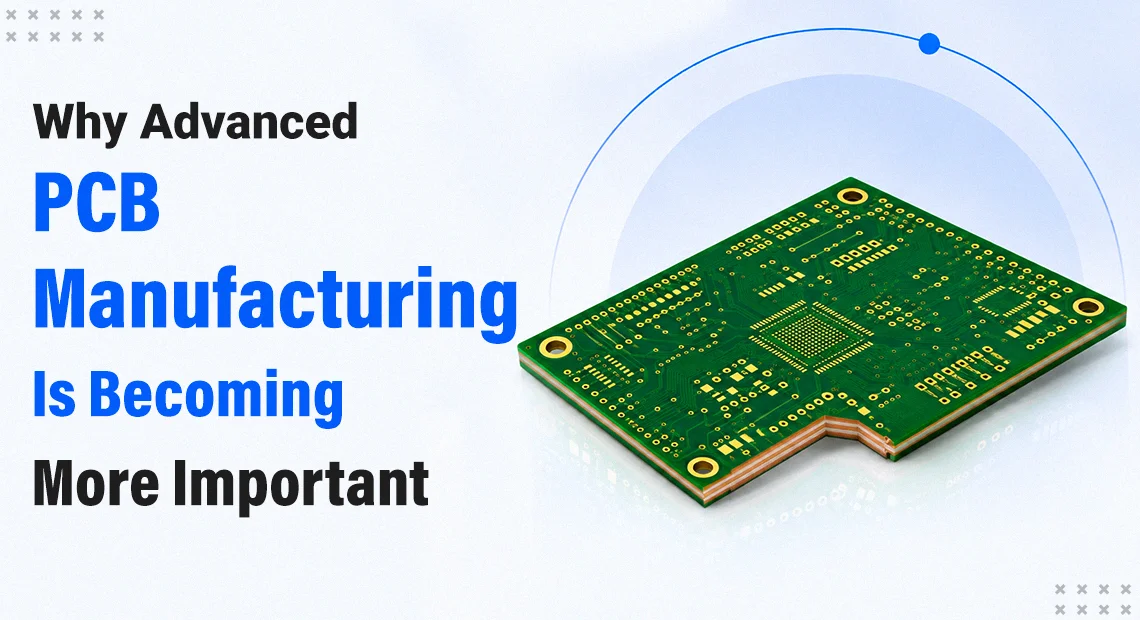
Advanced PCB manufacturing has importance given that modern electronics ask one board to carry a greater number of layers, faster signals, higher currents and tighter reliability targets at once. Four pressures drive this: density, signal speed, heat and the cost of failure. Defence, aerospace and medical boards feel all four, so process control and inspection decide the outcome.
A board that passes a bench test can still fail inside a vibrating airframe or a satellite subsystem nobody can reach. Layouts keep getting denser, while the tolerance for a misregistered layer or a thin plated barrel keeps shrinking.
That pressure drives the importance of advanced PCB manufacturing. PC Process, a PCB manufacturer in India operating from Peenya, located in Bengaluru, has been operating since 1983 and manufactures boards up to 24 layers. This post covers what is driving demand and what it asks of a manufacturer.
What advanced PCB manufacturing means in practice
Advanced PCB technology is defined by what the process can hold: registration, impedance, copper thickness and via structure, to the values the design depends on. That covers:
- High layer counts with consistent lamination and registration
- Controlled impedance routing
- Blind and buried vias
- Heavy copper for high-current paths
- Rogers and FR4 substrates, with ENIG or HASL finishes
Laser Direct Imaging (LDI) writes outer-layer patterns directly from data, which removes film registration error and holds accuracy below 25 µm.
Four pressures behind the importance of advanced PCB manufacturing
Each pressure changes a different manufacturing parameter.
Density: Shrinking components and growing I/O counts call for additional layers to separate power, ground and signal planes. Lamination cycles and registration across the stack become the controlling factors.
Speed: At fast edge rates a trace behaves as a transmission line. Impedance tolerances commonly sit at ±10%, so trace width, dielectric thickness and copper profile must be controlled together.
Heat: EV and industrial drives push current through heavy copper, which spreads heat but is harder to etch and laminate evenly.
Consequence: In a flight computer, radar module or imaging system, failure costs a programme or a patient outcome. That sets the reliability target before the first layer is drawn.
Where boards fail. During lamination, inner layers can move out of alignment, which shrinks the annular ring and weakens the connection between a via and its inner pad. Resin flow can also shift dielectric thickness, which moves impedance away from its target. Deep holes can end up with thinly plated barrels. Advanced PCB manufacturing addresses each of these through registration control, stack-up planning that accounts for prepreg behaviour, and plating thickness checks.
High layer count PCB applications
High layer count PCB applications concentrate where function density and signal integrity rise together: avionics and telemetry in aerospace, radar and secure communications in defence, switching and backplanes in telecom, imaging and monitoring in medical electronics, and drives and motion control in industrial automation.
Why PCB quality matters in defence and aerospace electronics
These boards operate through repeated temperature swings and vibration over long service lives, and field repair is often unavailable. Via barrels that crack under thermal cycling are a well-known failure mode, which is why plating thickness and drill quality receive close attention during qualification.
Production at PC Process is 100% in-house from DFM review to final test, so material lots, process parameters and test results trace to a single record. We hold ISO 9001:2015 and LCSO certification under JSS 52302, the Indian defence supplier standard, and our customers include HAL, BEL and ISRO (via VSSC).
High reliability PCB manufacturing starts with 100% inspection
Sampling infers lot quality from a handful of boards; 100% inspection gives every board its own result. Each unit passes automated optical inspection, fly probe testing, impedance measurement and CMI thickness checks. That record gives a quality manager something to audit.
Choosing a PCB manufacturing company for advanced boards
Buyers comparing advanced PCB manufacturers in Bangalore usually weigh four points:
- Layer count and material range
- Process steps held in-house
- Inspection scope: every unit or a sample
- Sector certifications
Prototype work deserves attention too. The prototype stage validates stack-up, impedance targets and via structure, and a prototype PCB manufacturer in Bangalore that also runs low-volume production keeps the process consistent between the first board and the hundredth. Bengaluru hosts many of India’s aerospace, defence and space organisations, and Peenya sits within the city’s industrial belt, so design and manufacturing teams can sit down together when a stack-up needs a decision.
Frequently asked questions
1. What is advanced PCB manufacturing?
Advanced PCB manufacturing covers boards with high layer counts, controlled impedance, blind and buried vias, heavy copper or RF laminates, built to tight registration and thickness tolerances through precise imaging,
2. Why is advanced PCB manufacturing becoming important?
A single board today has to handle dense routing, fast signals, high currents and demanding reliability targets together. Each of these tightens a manufacturing tolerance, which means registration, impedance and plating have to be controlled to narrower limits than standard boards call for.
3. What does advanced PCB technology include?
It includes multilayer stack-ups, controlled impedance routing, blind and buried vias, heavy copper, Rogers RF laminates and finishes such as ENIG and HASL, supported by Laser Direct Imaging for fine outer-layer accuracy.
4. Which industries rely on high-layer-count boards?
Aerospace and space research, defence, telecom and IT, medical electronics, automotive, industrial automation and research institutions use high layer count boards where routing density and signal integrity both matter.
5. How does high-reliability PCB manufacturing differ from standard production?
It verifies every board, controls plating, registration and impedance to the design’s limits, and keeps a traceable record of materials and test results for each order.
6. Why does PCB quality matter in defence and aerospace electronics?
Boards in these systems face thermal cycling, vibration and long service lives, and many sit out of reach once deployed. A single cracked via or misregistered layer can disable a unit, so process control and traceability carry real weight.
7. What layer count can PC Process manufacture?
PC Process manufactures multilayer PCBs up to 24 layers in FR4 and Rogers substrates, with blind and buried via structures and ENIG or HASL surface finishes.
8. What certifications does PC Process hold?
PC Process holds ISO 9001:2015 and LCSO certification under JSS 52302, the Indian defence supplier standard.
9. What should I check when comparing advanced PCB manufacturers in Bangalore?
Check layer count and material range, which steps happen in-house, whether inspection covers every unit, sector certifications and the engineering input offered before production. A PCB manufacturing company with in-house production keeps one record from design review to final test.
10. Is PC Process a prototype PCB manufacturer in Bangalore?
Yes. PC Process manufactures prototype and low-volume multilayer boards at its Peenya facility, with fast-turn and quick-turn options for urgent projects.


